How does processor read BIOS from SPI flash?
Asked Answered
D

1

10

A typical x86 systems has firmware (aka BIOS or UEFI) stored in a SPI based Flash chip. When the power-on happens, the processor starts executing at Reset Vector which is pointing to memory-mapped SPI chip where BIOS is stored. From here onwards, the bootstrapping happens when the BIOS finishes initalization of platform, loads the bootloader, which then loads the kernel.

However, how does the processor know how to read from the SPI chip? I mean, at that point processor will not be knowing about SPI protocol, which registers of chip to write command and which register to find the data read. How does the read happen at such low level?

Dionysian answered 13/2, 2020 at 5:3 Comment(2)
The hardware (in the southbridge) that maps physical addresses to different devices does know how to talk to SPI devices. I assume there's some way for the mobo vendor to set initial power-on state of address ranges, or that's hard-wired into the chipset. X86 Address Space Controller? may be relevant.Coronagraph
As Peter said, the PCH steers a window of memory to the SPI, with subtractive decoding. Maybe later I can find some time to write a proper answer.Flinty
F
21

The first thing a Haswell+ CPU does on power-up (after the BIST - Built-In Self Test) is executing a microcoded routine, part of Intel TXT technology, to fetch the FIT at 4GiB-40h and executes the BIOS ACM (Authenticated Code Module), and eventually continue the measured boot, or the fallback to the legacy reset vector at 4GiB - 10h.

Either way, the CPU needs to fetch instructions from a memory window a few MiB just below 4GiB.
The CPU doesn't have SPI interface, requests to this window are always redirected to the DMI interface, for security reasons.
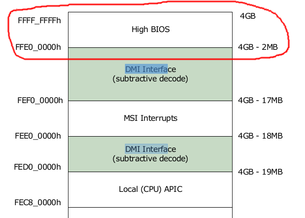
You can find the following map on Chapter 2.6 of the 8th-9th generation datasheet Vol. 2 (it is true even in previous generations, AFAIK):

Memory map

which is relevant due to this paragraph:

For security reasons, the processor will positively decode this [High BIOS] range to DMI. This positive decode ensures any overlapping ranges will be ignored. This ensures that the boot vector and BIOS execute off the PCH.

So the CPU boots off the DMI interface, and hence the PCH (Platform Controller Hub) handles the requests.
Note that even in older systems, where that near-4GiB window was subtractively decoded to the DMI interface (i.e. send to the DMI interface only if no other device claimed it), the boot was almost always from the DMI interface itself.
The new positively decoded behavior is a security measure against boot attacks.

If you look at the datasheet of a relatively modern PCH, i.e. series 200, you see that it supports a Flash ROM behind either the LPC bridge or the SPI interfaces.

We will restrict ourselves to the latter.
In that chipset the SPI bridge is the PCI device 31, function 15.
In its PCI configuration space there are the standard registers and:

  • A BAR (Base Address Register) to map a 4 KiB window of MMIO register to control the SPI interface itself.
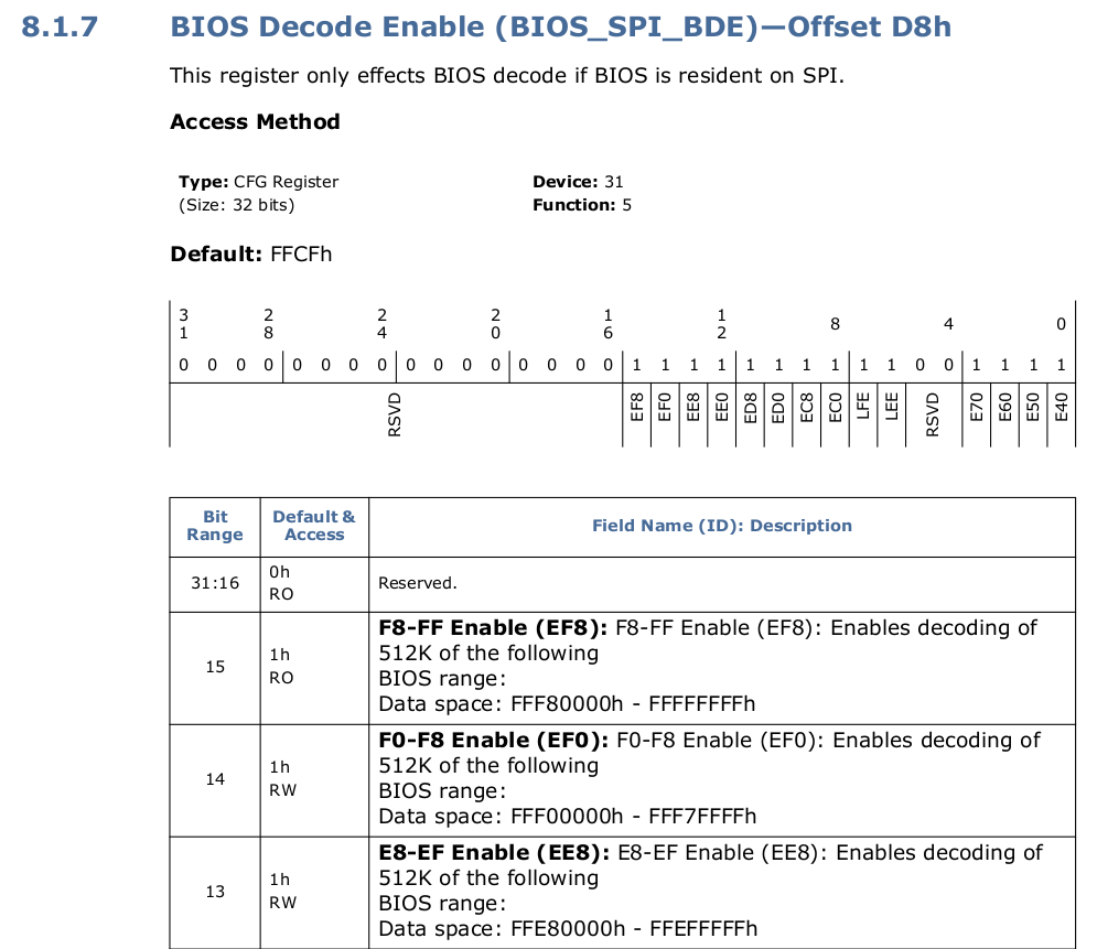
  • A BIOS Decode Enable register that enables or disables the reclaiming of the memory access in specific windows.
  • A control register to enable various security features (including if the boot is off the SPI or LPC interface).

Let's focus on the second point:

BIOS Decode Enable Register

Two things to note: first this register either enable or disable sending the memory accesses from the CPU, in the region of 4MiB below 4GiB and others, to the SPI.
The second is that the default value is 0ffcfh, meaning that by default all the windows are mapped to the SPI.
The BIOS Control Register also selects the SPI as the default boot interface but this is also configurable with softstrap/bootstrap pins, IIRC.

Last but not least, when the PCH sees an access to an address like 4GiB-10h it cannot send it as it to the Flash ROM as it would be out of range for the Flash ROM itself.
It must first decode it, subtracting an offset. However, this offset depends on the size of the Flash ROM.

Before the PCH (I think around the ICH8 chipset and in some non-too-recent Atom chipsets) the Flash ROM was used without descriptors.
The chipset simply mapped the ROM from the 4GiB down to 4GiB-16MiB with alias, meaning that the address 4GiB - X would be mapped to Flash Size - (X % Flash size).
The effect was that, e.g., a 2 MiB flash appeared mapped 8 times in the 16MiB windows below the 4 GiB limit.
In those chipsets there were bootstrap pins to configure the Flash Size.

Today Flash ROMs for the PCH use descriptors, where the flash is divided into regions (The BIOS, the ME, the GbE, etc.).
Only the BIOS region is mapped in CPU's address space. There is a system of security descriptors based on the id of the requester (given by its PCI identity).
For an introduction to this topic see this or better this for a more complete description (a bit outdated but still relevant).
Regions are relevant here because they are listed in the Flash descriptor with their offset and size, so the PCH can know how to translate the CPU addresses into the Flash Linear Addresses.

Finally, the MMIO registers of SPI interface allow for raw access to the Flash ROM. It is possible to synthesize commands to send down the SPI bus, making it possible to reprogram the Flash ROM (for example).
They are still subject to various security countermeasures that should be listed in the datasheet, IIRC.

Flinty answered 13/2, 2020 at 10:36 Comment(15)
trmm.net/Bootguard you might like this. I checked -18h on my physical memory dump and the pointer wasn't there so it's probably at xxC0 like it says. I need to check later. xxF0 had a relative jump to FFFFFFF5 - 3BD which had the following code: imgur.com/a/vy0LT5sIndian
Ok, it was at FFFFFFC0. Pointer to FFD90100. imgur.com/a/V5zhRS9Indian
@LewisKelsey Thank you, I've found sources with -18h and -40h, I checked which one was right but then forgotten about it. I'm editing the answer.Flinty
the SGX paper was the one that said FFFFFFE8 I think but I haven't seen it elsewhere. Anyway, I just realised the F0000–FFFFF region isn't mapped to the same part of the SPI ROM as FFFF0000–FFFFFFFF which any memory map diagram I've seen doesn't make clear and I'm sure I've seen 'alias' and things like that but actually, the routine jumped to by FFFFFFF0 expects es:[ffff0] (es = f000, where the segment descriptor has a 0 base) to contain a different reset vector, which on my system is an absolute 16 bit memory-direct direct unconditional far jump (EA opcode)Indian
I don't remember anything that could allow selecting how to map FFFF0 to the SPI ROM (but there may be something either in the FLASH descriptor or some bootstrap flag). The TOS Swap mechanism is used to do something similar, I would have to brush up on that. If you dumped the memory on a running system you may be dumping the shadowed firmware. Have you tried translating the target of the jump at FFFFFFF0 to its corresponding location in the upper SPI ROM? It is worth investigating, as soon as I found some time, I'll take a look at it. But i'd like a real SPI dump with a programmer :/Flinty
The bios decode enable register for SPI and LPC has a bit BIOS_LEGACY_F_EN for the F0000-FFFFF range. I assumed the reason for the difference was obviously that I could be reading shadowed code at this stage, but then I saw the code that I sent in the link above and it checks for the 0xeaf000e05b sequence at es:[ffff0] and if it matches it sends a '1' debug code to the POST code 0x80 port, skipping the test on the BSP bit in the APIC_base MSR. I'm not really sure what the purpose of this is but maybe it is checking to see whether it has already been shadowedIndian
But that doesn't make sense because it won't be at this stage. So that's why I began to think perhaps it's checking to see whether the actual memory map is correctIndian
@LewisKelsey It could simply be handling a warm reset or a check due to how the firmware is developed by the sw house.Flinty
You're right. I just ran the code through google search. github.com/andreiw/lampone-edk2-platforms/blob/master/Platform/…Indian
I saw the 67 prefix byte but I'm not sure why it's used here. (I'm not sure whether 67h sign extends or zero extends a moffs; I would have thought it zero extended, so it seems pointless). So it could be loading from 0xfffffff0h here, but I don't think it is, and I think that the 32 bit offset cannot exceed 64k in real mode, so again, pointless.Indian
@LewisKelsey Good finding! The 67h prefix doesn't extend (nor sign nor zero), it increases the width of the offsets in the instruction encoding. You can see that FFF0 is actually using four bytes. I think this is due to the developers using a 32-bit constant (and the assembler either didn't complain and emitted a 67h or warned and emitted it anyway).Flinty
Oh yeah. It was there in the instruction. I've worked it out partially. If EA is at FFFF0h then it checks FFFF1h for that ptr16:16. If it's there then it knows the shadowed ROM is present (I.e. some sort of soft reset e.g. INIT# occurred, which didn't affect the SPI flash), it then checks for the BSP flag, and if its the BSP, it jumps to the shadowed ROM at FFFF0h. If ptr16:16 isn't there, it jumps to the 16 bit + 32 bit protected mode setup (called 'nowarmstart'), which then jumps to 32 bit flat protected mode PEI implementation at 0x18:0xffffff6e.Indian
I don't know why EA would be there and that specific ptr16:16 wouldn't be, but apparently this results in a proper boot (jump to nowarmstart). If EA is not present, it checks bit 3 of 0xcf9 for 'Check INIT# is asserted'. If it is asserted then it performs a hard reset, writing 0x6 which results in a PLTRST#, reason 'issue warm reset, since if CPU only reset is issued not all MSRs are restored to their defaults'. If it isn't asserted then it jumps to 'nowarmstart'. reset types: chromium.googlesource.com/chromiumos/third_party/coreboot/+/…Indian
I'm not sure I understand that scenario where INIT# would be being asserted at that specific particular time. There is no documentation on reading from 0xcf9 like that. I'm amalgamating a UEFI answer to address what I know so far https://mcmap.net/q/546092/-how-does-uefi-workIndian
#54274721 I just found this.. (other suggestions in this matter) I guess I've got my work cut outIndian

© 2022 - 2024 — McMap. All rights reserved.